NANO-ERF® Series
Overview
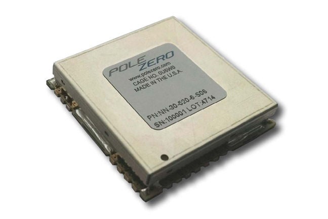
Product SKU ID:
Product Name: NANO-ERF® Series
The NANO-POLE® Extended Range Series of tunable filters was developed to address applications needing an extremely small surface-mount package with low power consumption. Wide tuning range is accomplished with careful design to minimize size and power consumption.

MODULAR
SWaP
CUSTOM DESIGN
Applications
Pole/Zero's RF Mixed Technologies Filters are tailored to end-user specifications and designed to meet custom needs across a number of industries, including the following markets: defense, EW, radar, communications, satcom, telecom, SIGIN, aerospace, space, automated test equipment, navigation/GPS and data links.
Markets

Product Specifications
Absolute Maximum Ratings
| Symbol | Parameter | Conditions | Min | Max | Unit |
| VCC | Supply voltage | - | -0.3 | 3.6 | V |
| VBB | High supply voltage | - | - | 28 | V |
| VI | Input voltage | On all digital interface input pins | -0.3 | 3.6 | V |
| VO | Output voltage | On all digital interface output pins | -0.3 | 3.6 | V |
| IOH/IOL | Digital interface pin sink/source current | - | -15 | 15 | mA |
| IO | Output current | - | - | - | mA |
| PINBAND | In-band RF input power level | Signal is in passband 𝑓0 = 30 − 520 𝑀𝐻z | - | 13^4 | dBm |
| POUTBAND | Out-of-band RF input power level | - | - | 20 | dBm |
| TRATE | Maximum tune rate (frequency hopping) | - | - | 2 | kHz |
Handling Ratings
| Symbol | Parameter | Conditions | Min | Max | Unit |
| TS | Storage temperature | - | -40 | +125 | °C |
Recommended Operating Conditions
| Symbol | Parameter | Conditions | Min | Nom | Max | Unit |
| VCC | Supply voltage | - | 3.315 | 3.3 | 3.6 | V |
| Vbb | Digital supply voltage | - | 23.75 | 25 | 26.25 | V |
| Pin | Maximum RF input power for linear operation | Signal is in passband | - | - | 6 | dBm |
| TA | Ambient temperature | - | -40 | - | +85 | °C |
Electrical Characteristics
| Symbol | Parameter | Conditions | Min | Nom | Max | Unit | |
| VCC | Supply voltage | At nominal Vcc voltage | 3.135 | 3.3 | 3.6 | V | |
| ICC_STATIC | VCC current consumption, statically tuned | At nominal VCC voltage | - | 3.3 | 30 | mA | |
| ICC_HOP | VVCC current consumption, hopping | Nominal VCC, hopping at - | - | - | - | mA | |
| VBB | High supply voltage | At nominal VBB voltage | 23.75 | 25 | 26.25 | ||
| IBB_STATIC | VBB current consumption, statically tuned | At nominal VBB voltage | - | - | 2 | mA | |
| IBB_HOP | VBB current consumption | Nominal VBB, hopping at - | - | - | - | mA | |
| VIH | Digital high level input voltage | On all digital interface input pins | 0.7* Vcc | - | - | V | |
| VIL | Digital low level input voltage | On all digital interface output pins | - | - | 0.3* Vcc | V | |
| IIH/IIL | Digital Interface pin input logic current | - | -10 | - | 10 | mA | |
| F(RANGE) | Tunable frequency range | - | 30 | - | 520 | MHz | |
| ZO | Input/output impedance | - | - | 50 | - | Ω | |
| VSWR | Voltage Standing Wave Ratio | - | - | 1.5:1 | 2.2:1 | - | |
| RL | Return loss | At 50 Ω | 8.5 | 14 | - | dB | |
| IL | Insertion loss | For NN-30-520-6-S06 | - | 4.7 | 7 | dB | |
| For NN-30-520-10-S06 | - | 3.2 | 5 | ||||
| %BW | Bandwidth (3 dB) | For NN-30-520-6-S06 | - | 6.5 | 7 | % | |
| For NN-30-520-10-S06 | - | 9.5 | 11 | ||||
| SEL15% | Selectivity 15% | 𝑓𝑂 ± 15% | 6%BW | - | 22 - | - | dBc |
| removed from the | |||||||
| center frequency | 10%BW | - | 17 | - | |||
| SEL(ULTIMATE) | Ultimate selectivity | 2 × fo | - | 50 | - | dBc | |
| IIP3 | Input third order intermodulation intercept point | - | - | 16 | - | dBm | |
| NF | Noise Figure | - | - | 8^6 | dB | ||
| Noise Floor | - | - | -100^7 | -85^7 | dBm | ||
| PSpurious | Spurious Output Level | - | - | -100^7 | -85^7 | dBm | |
| TTUNE | Tune time | - | - | 27 | 35 | μs | |
| FDRIFT | Center frequency drift over temperature | Fill in temperature range | - | 160 | 275 | ppm/°C | |
Resources
Pole/Zero ICE Product Catalog
BSC Filters Brochure
K&L Microwave Filters Product Catalog
Tunable Filters Brochure
Access Filter Wizard
Access QuEST
Featured Brand
Pole/Zero
Through continuous product, technology, and process innovation, Pole/Zero continues to expand its role as the leading supplier of unique, cost-effective solutions to the most complex of RF challenges. Our comprehensive suite of RF interference mitigation devices includes Tunable Filters, Low Noise Amplifiers, Integrated Cosite Equipment, Cosite Power Amplifiers and a wide range of other products tailored to the interference characteristics of multiple industries.
Our expertise and experience in space and military markets, has led to industry leading products that readily meet the unique size, weight and power requirements of cosite environments, placing us as a leading supplier for military applications.
Contact
Subscribe to receive all MPG updates.
SUBSCRIBE
REACH US AT
Microwave Products Group
13033 Trautwein Road
Austin, TX 78737
United States
Main: 410-749-2424
support@mpgdover.com
© COPYRIGHT ©2022, MPG - MICROWAVE PRODUCTS GROUP | A DOVER COMPANY | PRIVACY POLICY | COOKIES | TERMS OF USE