MAXI-POLE® Series
Overview
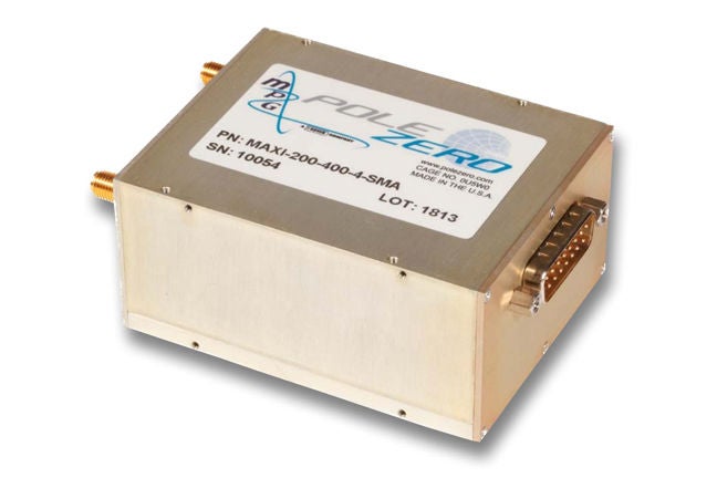
Product SKU ID:
Product Name : MAXI-POLE® Series

MODULAR
SWaP
CUSTOM DESIGN
Applications
Due to the durable packaging and high performance, Pole/Zero's Combline Filters are ideal for a variety of applications, including those in the following markets: defense, EW, radar, communications, satcom, telecom, SIGIN, aerospace, space, automated test equipment, navigation/GPS and data links.
Markets

Product Specifications
Absolute Maximum Ratings
| Symbol | Parameter | Conditions | Min | Max | Unit |
| VCC | Supply voltage | - | -0.5 | +6.0 | V |
| VBB | High supply voltage | - | - | +115 | V |
| VI | Input voltage on digital interface pins | Parallel Interface | -0.6 | +6.0 | V |
| Serial Interface | -0.5 | VCC + 0.5 | V | ||
| VO | Output voltage | On all digital interface output pins | -0.5 | VCC + 0.5 | V |
| PINBAND | In-band RF input power levelSignal is in passband 𝑓0 = 1.5 − 1000 𝑀𝐻z | Signal is in passband 𝑓0 = 1.5 − 1000 𝑀𝐻z | - | 33 | dBm |
| POUTBAND | Out-of-band RF input power level | - | - | 37 | dBm |
| TRATE | Maximum tune rate (frequency hopping) | 1.5 - 4 4 - 10- | - | 0.170 | kHz |
| 10 - 30 | - | 0.840 | kHz | ||
| 30 - 90 | - | 1.5 | |||
| 90 - 200 | - | 1.8 | |||
200 - 400 225 - 400 225 - 450 225 - 512 400 - 700 700 - 1000 | - | 2 |
Handling Ratings
| Symbol | Parameter | Conditions | Min | Max | Unit |
| Ts | Storage temperature | - | -40 | +85 | °C |
Recommended Operating Conditions
| Symbol | Parameter | Conditions | Min | Nom | Max | Unit |
| VCC | High Supply voltage | - | 4.5 | 5 | 5.5 | V |
| Vbb | Digital supply voltage | - | 90 | 100 | 110 | V |
| Pin | Maximum RF input power for linear operation | Signal is in passband | - | - | 30 | dBm |
| TA | Ambient temperature | - | -40 | - | 85 | °C |
Electrical Characteristics
| ICC_STATIC | VCC current consumption, statically tuned | At nominal VCC voltage | - | 80 | 250 | mA |
| ICC_HOP | VCC current consumption, hopping | Nominal VCC, hopping at 2 kHz | - | 80 | 250 | mA |
| IBB_STATIC | VBB current consumption, statically tuned | At nominal VBB voltage | - | 1 | 3 | mA |
| IBB_HOP | VBB current consumption | Nominal VBB, hopping at 1000 Hz | - | 9^7 | - | mA |
| VIH | Digital high level input voltage on all digital interface pins except STB ̅̅̅̅̅̅ | Parallel Interface | 2.0 | - | - | V |
| Serial Interface (-B) | 0.7 * VCC | |||||
| Digital high level input voltage on STB ̅̅̅̅̅̅ pin | All interfaces | 0.7 * VCC | ||||
| VIL | Digital low level input voltage on all digital interface pins except STB ̅̅̅̅̅̅ | Parallel interface | - | - | - | V |
| Serial interface (-B) | ||||||
| Digital low level input voltage on STB ̅̅̅̅̅̅ pin | All interfaces | |||||
| IL | Digital interface pin leakage current on all interface pins | - | - | - | 10 | µA |
| VOH | Digital high level output for serial interface (-B) | IOH = -400 µA | 2.4 | - | - | V |
| VOL | Digital low level output for serial interface (-B) | IOL = 2.1 mA | - | 0.4 | - | V |
| ZO | Input/output impedance | - | - | 50 | - | Ω |
| VSWR | Voltage Standing Wave Ratio | - | - | See Selection Guide | - | - |
| F(DRIFT) | Center frequency drift over temperature | -40 to +85 °C | - | - | -80 | ppm/°C |
| Weight | Weight of unit | - | - | 12 | - | oz |
Selection Guide
| Band | Suffix | 3 dB %BW | Insertion Loss (IL) (dB) | Return Loss (dB) | Shape Factor Overall (30 dB/3 dB ) | Selectivity (f0 ± 10%) (dB) | Ultimate Selectivity (2 * f0) (dB) | IIP3 (dB) | Noise Figure (dB) | ||||||
| Avg | Max | Avg | Max | Avg | Min | Avg | Max | Avg | Min | Typical | Avg | Avg | Max | ||
| 1 - 4 | 1 | IL | IL + 1dB | ||||||||||||
| 2 | 5.1 | 5.5 | 1.6 | 2.3 | 14 | 9.5 | 6.4 | 7 | 25 | 22 | 55 | 30 | IL | IL + 1dB | |
| 3 | IL | IL + 1dB | |||||||||||||
| 4 | IL | IL + 1dB | |||||||||||||
| 5 | 2 | 2.2 | 4.2 | 6.3 | 12 | 9.5 | 6.5 | 7 | 42 | 38 | 60 | 30 | IL | IL + 1dB | |
| 4 - 10 | 1 | IL | IL + 1dB | ||||||||||||
| 2 | 5.3 | 5.5 | 1.8 | 2.3 | 14 | 9.5 | 6.3 | 7 | 25 | 22 | 55 | 40 | IL | IL + 1dB | |
| 3 | 3.4 | 3.9 | 2.2 | 3.5 | 14 | 9.5 | 6.4 | 7 | 30 | 27 | 55 | 40 | IL | IL + 1dB | |
| 4 | IL | IL + 1dB | |||||||||||||
| 5 | 2 | 2.2 | 3.8 | 6.3 | 12 | 9.5 | 6.5 | 7 | 42 | 38 | 60 | 35 | IL | IL + 1dB | |
| 10-30 | 1 | IL | IL + 1dB | ||||||||||||
| 2 | 5 | 5.5 | 1.5 | 2.3 | 14 | 9.5 | 6.3 | 7 | 25 | 22 | 55 | 45 | IL | IL + 1dB | |
| 3 | 3.6 | 3.9 | 2 | 3.5 | 14 | 9.5 | 6.3 | 7 | 30 | 27 | 55 | 0.4 | IL | IL + 1dB | |
| 4 | 2.4 | 2.8 | 3.5 | 4.5 | 14 | 9.5 | 6.4 | 7 | 36 | 33 | 60 | 0.35 | IL | IL + 1dB | |
| 5 | 20 | 0.22 | 3.8 | 6.3 | 12 | 9.5 | 6.4 | 7 | 43 | 40 | 60 | 35 | IL | IL + 1dB | |
| 30 - 90 | 1 | IL | IL + 1dB | ||||||||||||
| 2 | IL | IL + 1dB | |||||||||||||
| 3 | 3.5 | 3.9 | 2.5 | 3.5 | 14 | 10 | 6.3 | 7 | 30 | 27 | 60 | 40 | IL | IL + 1dB | |
| 4 | 2.6 | 2.8 | 3.5 | 4.5 | 16 | 10 | 6.3 | 7 | 36 | 33 | 70 | 35 | IL | IL + 1dB | |
| 5 | 2 | 2.2 | 4 | 6.3 | 12 | 8 | 6.5 | 7 | 43 | 40 | 70 | 35 | IL | IL + 1dB | |
| 90 - 200 | 1 | IL | IL + 1dB | ||||||||||||
| 2 | IL | IL + 1dB | |||||||||||||
| 3 | 3.6 | 3.9 | 2 | 3.5 | 14 | 10 | 6.3 | 7 | 30 | 27 | 60 | 40 | IL | IL + 1dB | |
| 4 | 2.5 | 2.8 | 2.8 | 4.5 | 14 | 10 | 6.4 | 7 | 36 | 33 | 70 | 35 | IL | IL + 1dB | |
| 5 | 2 | 2.2 | 3.5 | 6.3 | 14 | 10 | 6.1 | 7 | 43 | 40 | 70 | 35 | IL | IL + 1dB | |
| 200 - 400 | 1 | 10 | 10.9 | 0.8 | 1.2 | 16 | 10 | 6.1 | 7 | 12 | 10 | 60 | 50 | IL | IL + 1dB |
| 2 | 5 | 5.5 | 1.6 | 2.3 | 14 | 10 | 6.1 | 7 | 25 | 22 | 60 | 45 | IL | IL + 1dB | |
| 3 | 3.4 | 3.9 | 2 | 3.5 | 14 | 10 | 6.2 | 7 | 30 | 27 | 60 | 40 | IL | IL + 1dB | |
| 4 | 2.5 | 2.8 | 2.8 | 4.5 | 14 | 10 | 6.3 | 7 | 36 | 33 | 70 | 35 | IL | IL + 1dB | |
| 5 | 1.9 | 2.2 | 4.2 | 6.3 | 12 | 8 | 6.3 | 7 | 43 | 40 | 70 | 35 | IL | IL + 1dB | |
| 225 - 400 | 1 | 10 | 10.9 | 0.7 | 1.2 | 16 | 10 | 6.1 | 7 | 12 | 10 | 60 | 50 | IL | IL + 1dB |
| 2 | 5 | 5.5 | 1.5 | 2.3 | 14 | 10 | 6.1 | 7 | 25 | 22 | 60 | 45 | IL | IL + 1dB | |
| 3 | 3.4 | 3.9 | 1.9 | 3.5 | 14 | 10 | 6.2 | 7 | 30 | 27 | 60 | 40 | IL | IL + 1dB | |
| 4 | 2.5 | 2.8 | 2.7 | 4.5 | 14 | 10 | 6.3 | 7 | 36 | 33 | 70 | 35 | IL | IL + 1dB | |
| 5 | 1.9 | 2.2 | 4.1 | 6.3 | 12 | 8 | 6.3 | 7 | 43 | 40 | 70 | 35 | IL | IL + 1dB | |
Resources
Pole/Zero ICE Product Catalog
BSC Filters Brochure
K&L Microwave Filters Product Catalog
Tunable Filters Brochure
Access Filter Wizard
Access QuEST
Featured Brand
Pole/Zero
Through continuous product, technology, and process innovation, Pole/Zero continues to expand its role as the leading supplier of unique, cost-effective solutions to the most complex of RF challenges. Our comprehensive suite of RF interference mitigation devices includes Tunable Filters, Low Noise Amplifiers, Integrated Cosite Equipment, Cosite Power Amplifiers and a wide range of other products tailored to the interference characteristics of multiple industries.
Our expertise and experience in space and military markets, has led to industry leading products that readily meet the unique size, weight and power requirements of cosite environments, placing us as a leading supplier for military applications.
Contact
Subscribe to receive all MPG updates.
SUBSCRIBE
REACH US AT
Microwave Products Group
13033 Trautwein Road
Austin, TX 78737
United States
Main: 410-749-2424
support@mpgdover.com
© COPYRIGHT ©2022, MPG - MICROWAVE PRODUCTS GROUP | A DOVER COMPANY | PRIVACY POLICY | COOKIES | TERMS OF USE