Maxi-Pole Notch Series
Overview
Product SKU ID:
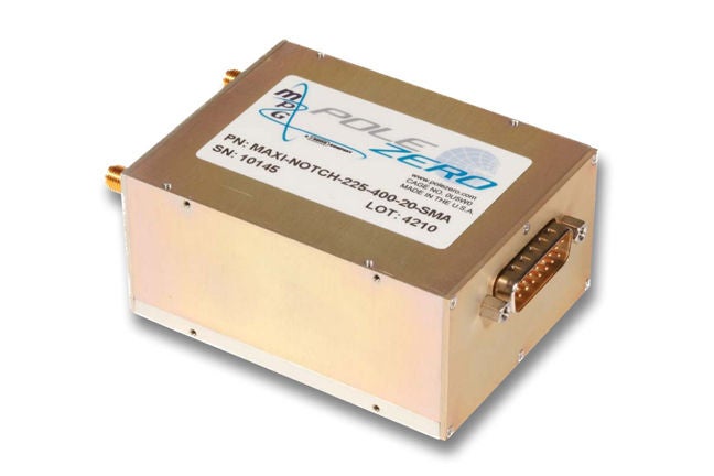
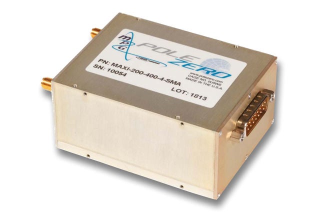
Product Name : MAXI-POLE® Notch Series
MAXI-POLE® Notch Filters offer all of the same performance features as the MINI-POLE® Notch filters, with the advantage of an improved notch shape factor.

MODULAR
SWaP
CUSTOM DESIGN
Applications
The low distortion and optimal RF power handling make Pole/Zero’s MAXI-POLE Filter applicable for multiple markets, including defense, EW, radar, communications, satcom, and automated test equipment.
Markets

About The Technology
Maxi-Notch®
Featured Brand
Product Specifications
| Frequency Coverage (5 bands): | Input/Output Impedance: | Inband RF Power Handling: | Passband Third Order Intercept Point: | Passband Insertion Loss: | Passband VSWR: | Tuning Control: | Tuning Speed: | DC Power: | Operating Temperature Range: | Center Frequency Drift: | |
| 1.5 MHz to 400 MHz | 50 Ω | 1 Watt (input) | +50 dBm (input,f0 > 30 MHz) | 1 dB (max) | 2:1 (max) | 8 bit parallel | 10 µ S (f0 > 30 MHz, | +10 dBm reference) | +5 VDC @ 10 to 500 mA +100 VDC @ 1mA | -40 to + 85°C | 80 PPM/°C |
Resources
Pole/Zero ICE Product Catalog
BSC Filters Brochure
K&L Microwave Filters Product Catalog
Tunable Filters Brochure
Access Filter Wizard
Access QuEST
Contact
Subscribe to receive all MPG updates.
SUBSCRIBE
REACH US AT
Microwave Products Group
13033 Trautwein Road
Austin, TX 78737
United States
Main: 410-749-2424
support@mpgdover.com
© COPYRIGHT ©2022, MPG - MICROWAVE PRODUCTS GROUP | A DOVER COMPANY | PRIVACY POLICY | COOKIES | TERMS OF USE